At the Applied Power Electronics Conference & Exposition (APEC 2022), power device manufacturers focused on giving system power designers more choices to help them select the right component for their application and higher integration to simplify complex power designs. They also delivered a greater selection of wide-bandgap (WBG) semiconductors, highlighting gallium-nitride (GaN) and silicon carbide (SiC) power devices for a range of automotive, communications, and industrial applications.
Other big power trends, in addition to improving efficiency and system complexity, include improved thermal management and smaller packaging. A common theme among these requirements is a need to lower bill of materials (BOM) costs, which is achieved by reducing the number of external components required in these system designs. This also often leads to higher efficiency and simplified designs.
At the same time, there is increasing demand for both SiC and GaN power devices. These devices offer inherent advantages over silicon, including higher bandgaps, lower conduction losses, and faster switching.
Here is a selection of power devices featured at APEC 2022 that deliver higher functionality, integration, and efficiency for a wide range of applications. There is also a sampling of new SiC and GaN devices.
High integration and high efficiency
Eggtronic has expanded its EcoVoltas family of high-efficiency AC/DC architectures with the new SmartEgg zero voltage switching (ZVS) PFC and regulator solution. The SmartEgg solution is designed for power applications in the 75 W to 1 kW range that need both output voltage regulation and power factor correction.

Click for a larger image. (Source: Eggtronic)
The ZVS solution is said to enable a much higher no-load-to-full-load efficiency. “Forced ZVS under every load condition delivers efficiencies of up to 95% at full load and 92% at light load,” said the company.
SmartEgg can achieve power densities of 30 W/in3, according to the company. The new architecture also delivers a 50 percent smaller BOM than conventional converters. It is also said to be one of the first platforms to support the new USB Power Delivery Revision 3.1 specification, delivering up to 240 W of power over full-featured USB Type-C cables and connectors.
SmartEgg consists of an input rectifier (solutions are based on either an input bridge or bridgeless rectifier), two primary FETs, two secondary FET rectifiers, a single magnetic component, and a few capacitors. The main controller manages PFC and output voltage regulation, ZVS, and frequency control.
Traditional medium-power AC/DC PFC architectures use a boost PFC input stage and an LLC stage that controls the output voltage, said Eggtronic. In comparison, the SmartEgg cuts the number of MOSFET and magnetic components in half by replacing these two stages with a single-stage converter capable of controlling both input current and output voltage.
Eggtronic can create custom designs based on the new SmartEgg architecture or can provide the reference design together with the IC controller. The first fixed-voltage reference design is available now.
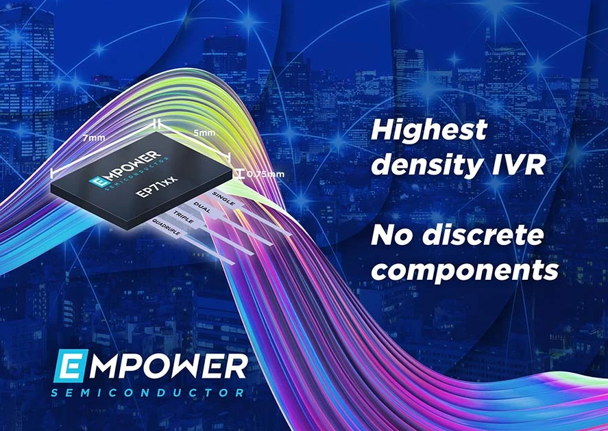
Empower Semiconductor, Inc. has introduced its first series of quad-output step-down converters to its family of integrated voltage regulators (IVRs) that combine high current density and efficiency, fast dynamic voltage scaling (DVS) and transient response, and fault protection. The new digitally configurable EP71xx series can deliver complete voltage regulation and protection functionality without the need for external discrete components, while reducing other system components and cost thanks to their high integration, said the company.

Click for a larger image. (Source: Empower Semiconductor)
The company said the new IVRs reduce PCB power management area and components by ten times or more, and cuts system power losses by as much as 50%, while simplifying system design.
IVRs, which are high-performance power management ICs, monolithically integrate the voltage regulator and all the necessary discrete components in a single device. The integration is said to simplify the design and implementation of voltage regulation circuitry, while improving the efficiency by eliminating connection losses and reducing susceptibility to EMI. This translates into a smaller bill of materials, higher reliability, and a reduced PCB footprint, said the company.
The EP71xx series delivers 12 A of continuous current with up to four voltage regulators in a single FcCSP package that measures 5 × 7 mm with a height of 0.7 mm. The IVR family operates from a single 3.3-V input and is comprised of a variety of devices that can provide the 12 A from one to four independent outputs. Output voltages are programmable from 0.5 V to 2.5 V and output voltage set-point accuracy is +/- 1.0%. Built-in fault protection and warning capabilities cover OVLO, UVLO, OVP, OCP, and short circuits.
The devices are said to provide ultra-fast transient response, which supports regulation through a load step, and the programmable ‘ExpressV’ DVS-on-demand is capable of up to 6 mV/ns. This feature is said to be more than 1000× faster than other competing technologies, enabling lossless, processor state changes that can significantly reduce processor power.
Murata has introduced the UltraCP MYC0409 , a 48 Vin divide-by-4 pump capacitor divider module with all passive components integrated in a low-profile (11.5 × 9.5 × 2.0 mm) PSiP package. The company claims the new DC/DC converter module offers the highest power density (5.4 kW/inch3), delivering 72 watts with peak efficiency of around 97 percent.

MYC0409 DC/DC converter module. Click for a larger image. (Source: Murata)
The module’s interleaved, switching capacitor architecture is based on Murata’s lossless charge pump technology that is said to provide extremely low input and output ripple performance.
The MYC0409 operates in a fixed divide-by-4 mode over an input voltage range of 20 V to 60 V, which extends its use to 24-V to 36-V input applications typically used in consumer battery charging and industrial supplies. The charge pump-based DC/DC converter supports an output voltage range of 5 V to 15 V with load currents of 6 A and up to 72 W delivered to the external load. The devices offer an extended temperature range of -40°C to 105℃. Protection functionality includes input undervoltage, overcurrent protection, and thermal shutdown fault detection.
The MYC0409 devices can be connected in parallel to provide high power and high efficiency solutions suitable for 48-V to 12-V step-down conversion applications such as data centers, networking routers, base stations, and optical equipment.
Traditionally, companies have used brick converters to step-down from 48 V to the intermediate bus, usually 12 V, said Murata. In comparison, the MYC0409 enables system architects to design high density, 48-V converters in a smaller footprint with enhanced efficiency and low ripple performance.
This means system designers can choose between creating a single high-power bulk 48-V bus system with MYC0409 devices connected in parallel or distributing individual MYC0409 devices close to the point-of-load, which reduces system PCB copper losses, said Murata.

HiperLCS-2 LLC switcher chipset. Click for a larger image. (Source: Power Integrations)
Power Integrations has launched an energy-saving HiperLCS-2 LLC switcher chipset that is designed to simplify the design of LLC resonant power converters. The surface-mount chipset delivers 250 with over 98% efficiency without a heat sink and no-load consumption of less than 50 mW.
The new dual-chip solution features an isolation device with a high-bandwidth LLC controller, synchronous rectification driver, and FluxLink isolated control link, together with a separate half-bridge with integrated 600-V FREDFETs with lossless current sensing and high- and low-side drivers. Both devices are housed in low-profile InSOP-24 packages. The FluxLink technology for digital feedback control also is said to provide a much faster transient response and improved long-term reliability compared to optocouplers.
This high integration architecture eliminates heat sinks and optocouplers, and reduces component count by up to 40 percent compared to discrete designs, while yielding 98% efficiency, said Power Integrations. The devices enable designers to create compact adapters and open-frame power supplies for TVs, monitors with USB PD ports, all-in-one PCs, game consoles, and battery chargers for power tools, and e-bikes, said the company.
With the HiperLCS-2 power supply designers can achieve no-load input power of less than 50 mW at 400 VDC input and provide a continuously regulated output, said the company, which allows for compliance with no-load and standby efficiency regulations.
The HiperLCS-2 devices feature self-powered start-up and provide the start-up bias for a PFC stage using the company’s HiperPFS ICs. The secondary-side sensing provides less than one percent regulation accuracy across line and load range and across production variations. A reference design, DER-672, is available to evaluate the HiperLCS-2 ICs.
TDK Corp. has introduced the FS1412, an ultra-low-profile microPOL (μPOL) power module, designed for space-constrained applications. The FS1412, measuring 5.8. × 4.9 ×1.6 mm, joins a new series of µPOL DC/DC converters with increased performance, small size, and simplified integration for applications such as big data, machine learning, artificial intelligence (AI), 5G cells, IoT networking, telecommunication, and computing enterprise, said TDK.

FS1412 μPOL DCDC converters. Click for a larger image. (Source: TDK Corp.)
The FS1412 μPOL DC/DC converters integrate a pulse-width modulation (PWM) controller, MOSFETs, an inductor, and capacitors. The μPOL technology enables the integrated DC/DC converters to be placed near complex chipsets such as ASICs and FPGAs.
The new µPOL DC/DC converter series operates at a broad junction temperature range from -40°C to 125°C. They feature a high current density of more than 1000 A per cubic inch. Built-in protection features include soft-start protection, over-voltage protection, thermally compensated over-current protection with hiccup mode, and thermal shut-down with auto-recovery. The devices are lead free and RoHS/WEEE compliant.
The series delivers 12 A with the lowest commercially available height at 1.6 mm, while offering 50% less solution size than the other products available in its class for lower cost and reduced board size, said TDK. Volume production for the FS1412 started in the fourth quarter of 2021.
Texas Instruments (TI) has launched three new power ICs, targeting automotive and industrial applications. The new products include the LMQ66430 and LMQ66430-Q1 buck converters and TPS7A94 low-dropout (LDO) linear regulator.

LMQ66430 buck converter. Click for a larger image. (Source: Texas Instruments Inc.)
The new 36-V, 3-A LMQ66430 and LMQ66430-Q1 buck converters are designed to lower electromagnetic inductance (EMI) in automotive and industrial applications while improving filter size. The devices integrate two input bypass capacitors and one boot capacitor. This enables engineers to meet Comité International Spécial des Perturbations Radioélectriques (CISPR) 25 Class 5 EMI standards while claiming a best-in-class total solution size of of 114 mm2, 1.5-µA quiescent current (IQ), and reduced bill-of-materials costs.
By integrating the three capacitors in a 2.6 × 2.6-mm enhanced QFN package, it allows for a super small solution, and the benefit to customers is a much smaller EMI passive filter, said Carsten Oppitz, vice president and general manager, buck switching regulators at TI.

TPS7A94 LDO linear regulator. Click for a larger image. (Source: Texas Instruments, Inc.)
Designed to enhance the power and signal integrity of low-voltage devices thanks to its low noise, the TPS7A94 LDO linear regulator claims the industry’s lowest noise of 0.46 µVRMS – at least 42% better than competing solutions – with a high power-supply rejection ratio (PSRR). This helps designers improve system accuracy and precision in highly sensitive applications.
The TPS7A94 also does not require additional filtering components, which make the design smaller and more cost efficient.
TI also demoed several system-level solutions at APEC, which covered increasing power density, reducing EMI, enabling safer systems, extending battery life, and enhancing the power and signal integrity of low-voltage devices. (For more details, please visit here.)
More choices for more applications
MaxLinear Inc. has introduced a new line of Intelligent point-of-load (iPOL) buck regulators for server, data center, networking, and wireless communications applications. The MxL76xxP series of step-down, synchronous regulators is comprised of four versions based on current ratings – 6 A, 12 A, 20 A, and 30 A).

Click for a larger image. (Source: MaxLinear)
The MxL76xxP family delivers control and monitoring of all voltage rails in a single chip solution by integrating the output power FETs, control loop and digital telemetry into a single small package. With the PMBus digital interface, the synchronous regulators support monitoring of input and out put voltage and current while enabling control of all setpoints.
MaxLinear said performance and system thermals are optimized by adjusting the output on the fly as required with modern CPUs/ASICs using dynamic voltage scaling (DVS).
The devices operate from 3-V to 16-V inputs, supporting both data center distribution rails and PCIe cards. The integrated synchronous FETs rated for 6 A, 12 A, 20 A, or 30 A allow the right device to be selected for the application, optimizing the efficiency and cost of the solution, said MaxLinear. In addition, with the MaxLinear PowerArchitect GUI, the entire setup, control and monitoring of a design can be completed without external design components, which reduce development time and design complexity.
Samples can be ordered for the MxL7630P, MxL7620P, MxL7612P, and MxL7606P, with output current ratings of 30 A, 20 A, 12 A, and 6 A, respectively . They are available in 4 × 5.5 mm, 4 × 4.5 mm, 4 × 4 mm, or 4 ×3.5 mm QFN packages.
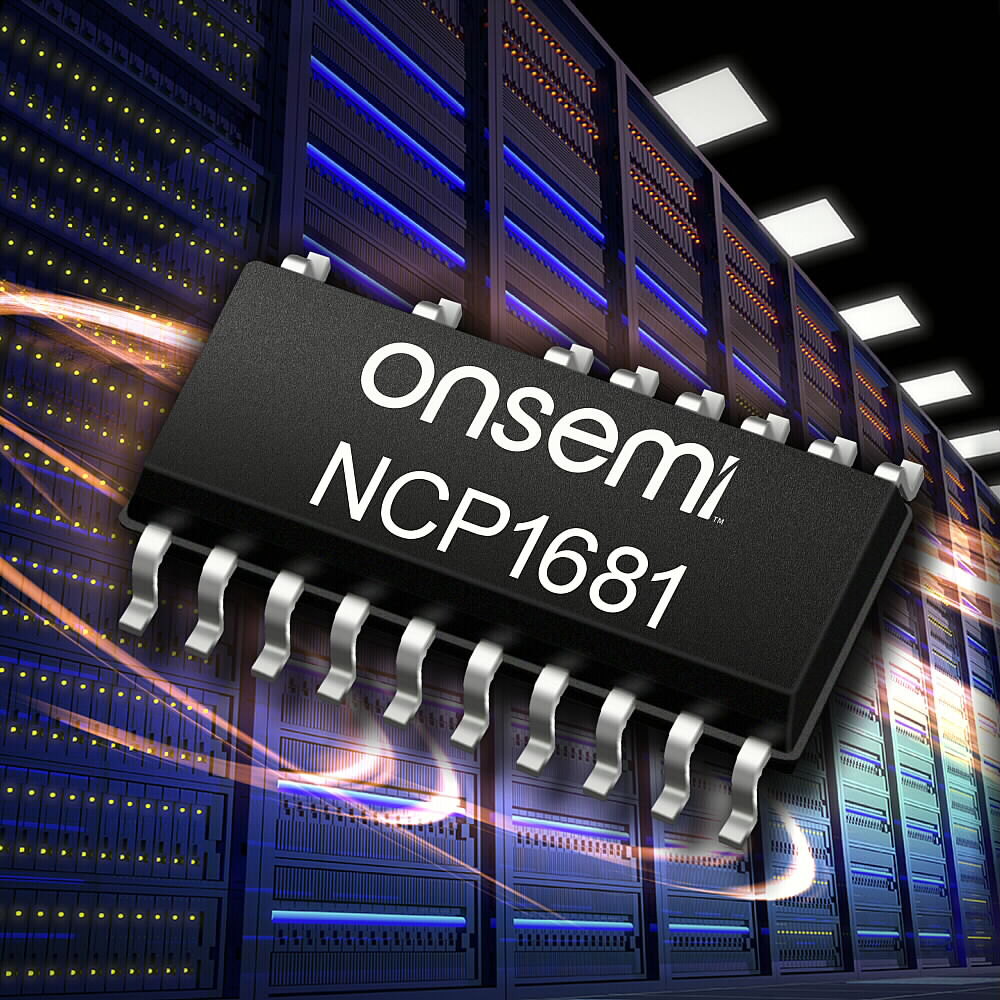
Onsemi has introduced a new high-power totem pole PFC (TP-PFC) controller that reduces development time and cost. Joining the NCP1680, which is suited for designs up to 350 W, the new NCP1681 extends the power capability into the kilowatt range, targeting ultra-high-density offline power supplies.

Click for a larger image. (Source: onsemi)
The NCP1681 is designed to drive the bridgeless totem-pole PFC topology. This topology eliminates the diode bridge used at the input of a conventional PFC circuit, allowing significant improvement in the power stage efficiency, said onsemi.
TP-PFC designs typically require an MCU that added design complexity and the need for coding, said onsemi, but with the NCP1681, it doesn’t require coding and only a few external components are needed for a fully-featured TP-PFC solution.
The NCP1681 can be configured to work in either fixed frequency continuous conduction mode (CCM) or multi-mode operation, where the controller transitions between CCM and critical conduction mode (CrM) for optimal performance across power levels, said the company.
The NCP1681 is suited to higher-power power supplies from 350 W to several kilowatts that operate on universal mains input (90 – 265 VAC). This makes them suitable for a wide range of applications including servers, high performance computing, telecom, industrial, and OLED TVs. At high line, the NCP1681 TP-PFC solutions will achieve close to 99% efficiency. These devices can meet efficiency standards such as 80Plus and CoC Tier 2.
WBG power devices
Infineon Technologies AG has expanded its CoolSiC family with a new line of 650-V SiC MOSFETs in a compact D2PAK 7-pin package with .XT interconnection technology. Comprised of 10 new products, these SiC MOSFETs can be used in a range of power applications, including servers, telecom, industrial SMPS, fast EV charging, motor drives, solar energy systems, energy storage, and battery formation.
The .XT interconnection technology is said to significantly improve the package’s thermal capabilities. Infineon said up to 30 percent extra loss can be dissipated compared to a standard interconnection.

Click for a larger image. (Source: Infineon Technologies)
The new SiC products claim improved switching behavior at higher currents and 80 percent lower reverse recovery charge (Q rr) and drain-source charge (Q oss) than the best silicon reference. The reduced switching losses allow high-frequency operations in smaller system sizes, enabling higher efficiency and power density, said Infineon, with the trench technology contributing to the higher gate oxide reliability. The devices also provide improved avalanche and short-circuit robustness for high system reliability.
The SiC MOSFETs are suitable for topologies with repetitive hard commutation as well as for high temperature and harsh operations. They also are said to deliver excellent thermal behavior thanks to a very low on-resistance, or RDS(on).
The new family also works with standard MOSFET gate driver ICs thanks to a wide gate-to-source (V GS) voltage range from -5 V up to 23 V, 0 V turn-off V GS, and a gate-source threshold voltage (V GS(th)) greater than 4 V. The devices support bi-directional topologies and full dv/dt controllability, which provides several benefits, including reduced system cost and complexity, as well as ease of integration.

Click for a larger image. (Source: Microchip Technology)
Microchip Technology Inc. also has expanded its silicon carbide (SiC) portfolio with the introduction of 3.3-kV SiC MOSFETs and SiC Schottky barrier diodes (SBC), claiming the industry’s lowest on-resistance 3.3-kV SiC MOSFETs and highest current-rated SiC SBDs available in the market. These devices target high-voltage power electronics in electrified transportation, renewable energy, aerospace, and industrial applications. These include traction power units (TPUs), auxiliary power units (APUs), solid-state transformers (SSTs) industrial motor drives, and energy infrastructure solutions.
Until now the availability of 3.3 kV-SiC power devices has been limited. Joining Microchip’s SiC family that includes 700-V, 1200-V and 1700-V products, the five initial 3.3-kV devices include three MOSFETS that offer 25 mOhm to 400 mOhm on-resistance, or RDS(on), with rated current of 104 A, 43 A, and 8 A, and two SBDs rated at 30 A and 90 A. Microchip claims the new 3.3-kV SiC MOSFETs provide the industry’s lowest on resistance at 25 mOhm and the SBDs offer the industry’s highest current rating of 90 amps. The 3.3-kV MOSFETs and SBDs are available in die or package form.
As part of the company’s focus on ruggedness, performance, and reliability, the SiC devices deliver very high gate oxide integrity (100+ years), degradation-free and robust body diodes, as well as strong avalanche ruggedness, delivering stable performance after 100K pulses, and short-circuit protection. The 3.3-kV SiC MOSFETs and SBDs are available in die and package options. (For more details, please visit here.)
Power Integrations has launched the HiperPFS-5 family of power-factor-correction (PFC) ICs with an integrated 750-V PowiGaN gallium-nitride (GaN) switch. The quasi-resonant PFC ICs deliver an efficiency of up to 98.3 percent and up to 240 W without a heat sink.
The PFC ICs also can achieve a power factor (PF) of better than 0.98. At light load, the HiperPFS-5 ICs are said to maintain a high PF of 0.96 even at 20 percent load. No-load power consumption is 38 mW.

Click for a larger image. (Source: Power Integrations)
Suited for high-power USB PD adapters, TVs, game consoles, all-in-one computers, and appliances, the HiperPFS-5 PFC ICs with PowiGaN technology and a QR control scheme deliver a new solution for handling losses in the power line caused by capacitors and inductors used in power supplies that generate a phase change between the current and voltage.
The HiperPFS-5’s QR discontinuous conduction mode (DCM) control technique adjusts the switching frequency across output load, input line voltage, and input line cycle. Power Integrations said QR DCM control ensures low switching losses and allows the use of a low-cost boost diode. The low switching and conduction loss, together with lossless current sensing, is said to enable high efficiency across the entire load range.
In addition, the variable frequency engine allows the reduction of the boost inductor size by more than 50 percent compared to conventional critical-conduction-mode (CRM) boost PFC circuits, said PI.
HiperPFS-5 ICs maintain a high PF up to 305 VAC and can operate continuously at up to 460 VAC during line swells, said the company. They also incorporate the company’s automatic X-capacitor discharge (CAPZero) function, including the required redundant pins to meet safety regulations, and high-voltage self-start-up.
The HiperPFS-5 quasi-resonant PFC controller ICs, housed in a SOP-T28F SMD power package, are available now. The reference design DER-672 is available to download for evaluating the HiperPFS-5.

Click for a larger image. (Source: STMicroelectronics)
STMicroelectronics has released its VIPerGaN50 50-W gallium-nitride (GaN) flyback converter with an integrated 650-V GaN power transistor, delivering miniaturization and high energy efficiency to a range of consumer and industrial applications. These include power adapters, USB-PD chargers, and power supplies for home appliances, air conditioners, LED-lighting equipment, and smart meters.
The VIPerGaN50 is the first device in the VIPerPlus series to offer up to 50 W in a wide 9 V to 23 V operating voltage range. It is also ST’s first VIPer device with a GaN transistor. “The VIPerGaN50 helps designers leverage GaN wide-bandgap technology to meet increasingly stringent eco-design codes that target global energy savings and net-zero carbon emissions,” said STMicroelectronics.
With its single-switch topology and high integration, which includes built-in current-sensing and protection circuitry, the VIPerGaN50 also is housed in a compact 5 × 6-mm package. In addition, minimal additional external components are needed to design an advanced, high-efficiency switched-mode power supply (SMPS), and thanks to the speed of the integrated GaN transistor it allows for a high switching frequency with a small and lightweight flyback transformer, said the company.
The converter operates in multiple modes to optimize efficiency at all line and load conditions. At heavy load, quasi-resonant (QR) operation with zero-voltage switching minimizes turn-on losses and electromagnetic emissions (EMI), while at reduced load, valley skipping limits switching losses and leverages ST’s proprietary valley lock to prevent audible noise.
ST said the frequency foldback with zero-voltage switching ensures the highest possible efficiency at light load. It also uses adaptive burst mode operation to minimize losses at very low load. Advanced power management features reduce standby power to below 30 mW.
In addition to the built-in protection circuitry, including output over-voltage protection, brown-in and brown-out protection, and input over-voltage protection, input-voltage feedforward compensation is also included to minimize output peak-power variation, as well as embedded thermal shutdown and frequency jittering to minimize EMI.
TDK-Lambda, a group company of TDK, has expanded its GaN-based PFH500F AC/DC GaN power module family with two new models based on the Transphorm TP65H070LDG 72 mΩ GaN FETs in 8 × 8 PQFN packages. The new PFH500F-12 and PFH500F-48 are the second and third modules in TDK’s series of 500-watt AC/DC power supplies, providing 12-V and 48-V power outputs, respectively.

Click for a larger image. (Source: TDK-Lambda)
Like their predecessor, the GaN-based 28-V PFH500F-28, these new AC/DC GaN power modules deliver GaN benefits, including a six percent efficiency increase in a 13 percent smaller device package (from 116.8 × 61 mm to 101.6 × 61 mm). Together, these benefits translate into a 38 percent power density (> 100 W/in^3) improvement when compared to the PFE500SA-12 and PFE500SA-48, TDK-Lambda’s silicon-based 12-V and 48-V modules.
The new power modules also allow for the use of smaller external capacitors. They also add a PMBus interface with read/write capability for remote monitoring and programming. The operating temperature range is -40°C to 100°C.
The Transphorm power transistors’ high power density enabled TDK to cool the GaN power supplies via thin baseplates, enabling the power modules to support a variety of industrial applications operating in harsh environments, said Transphorm. Applications include commercial off-the-shelf (COTS) power supplies, custom fanless power supplies, 5G communication, laser, digital signage/displays, and signaling.